
Overview
Few years ago I was working on a simple VNA in the frequency range near DC up to 1MHz. The purpose of that was to analyze the feedback loop of analog circuits that were unstable, helping me determine the actual loop transfer function and fix it.
This method works by breaking the feedback loop in a specific point, injecting a small test signal with an injection transformer and determine magnitude and phase at every frequency by comparing the injected signal with the one that has travelled through the loop.
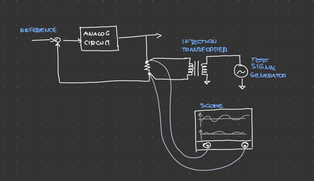
Since the amplitude of the injected signal must be low in order not to have too big of an influence on the feedback network (roughly 1-50mV), the signals that need to be analyzed are very low in amplitude and can be very noisy if the signal under test is a switching regulator or similar.
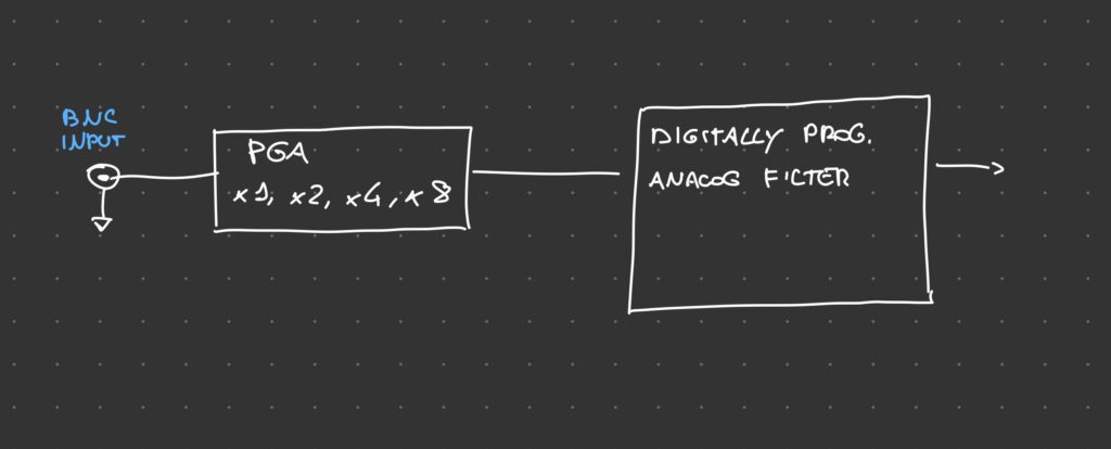
To take care of these weak signals this is the analog frontend implemented
Where Digitally Programmable Analog Filters Come Into Play
Very weak and noisy signals need special care. The first stage of the frontent is a Programmable Gain Amplifier that buffers and amplifies the incoming signal. The second stage is an analog filter of which cutoff frequency can be programmed digitally via I2C interface. The topology of this filter is the following
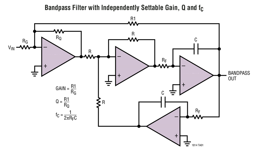
Which have many good chracteristics, like:
- allows to set independently gain, Q factor and cutoff ferquency (with other active filters modifying the cutoff frequency also modifies the Q factor)
- has both high-pass, lowpass (40dB/dec rollof) and bandpass (20db/dec rolloff) output responses
To make the filter digitally programmable, in place of C there are many capacitances that can be selected through an analog multiplexer, and in place of R there are two digital potentiometers.
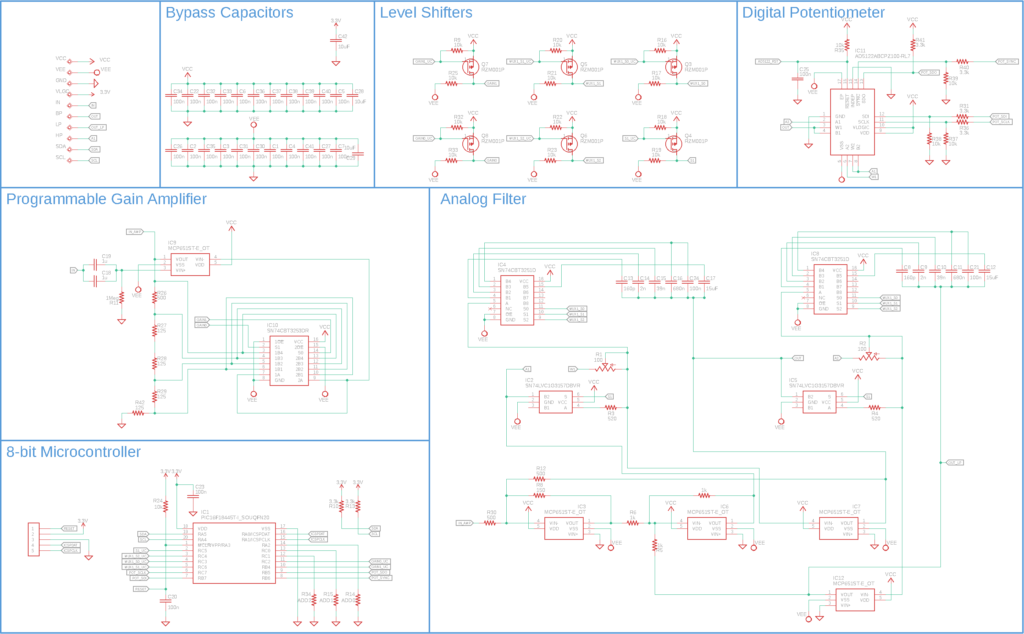
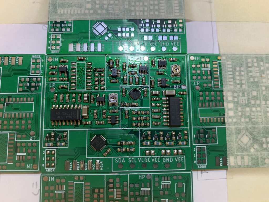
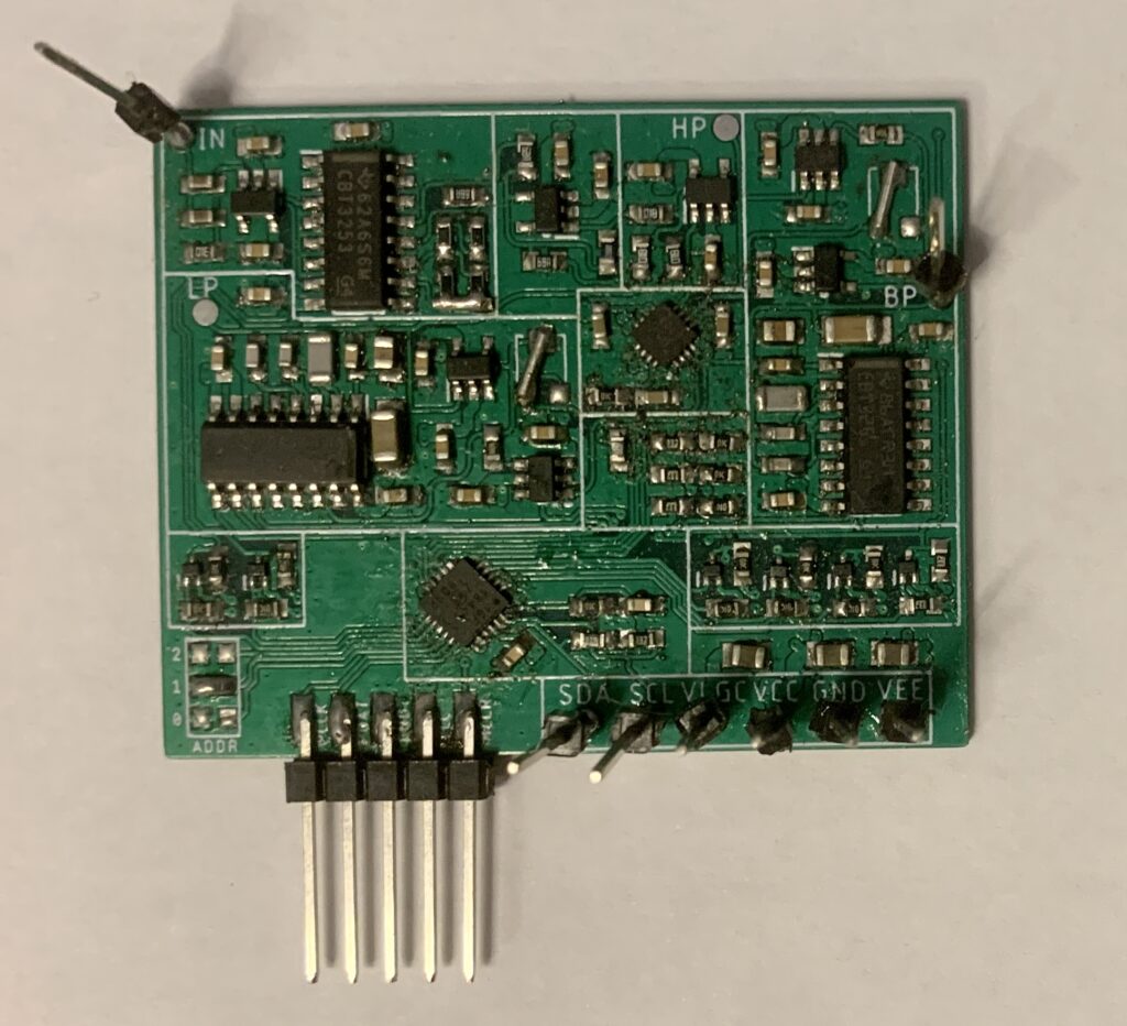
The board I have developed includes both the PGA and the programmable filters. The digital interface is controlled by a microcontroller (PIC16F1845) which controls the multiplexer and the potentiometer
Schematics
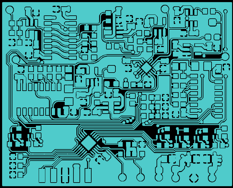
PCB
The PCB has a 4-layers stackup (SIGNAL – GND – POWER – SIGNAL)

Assembly
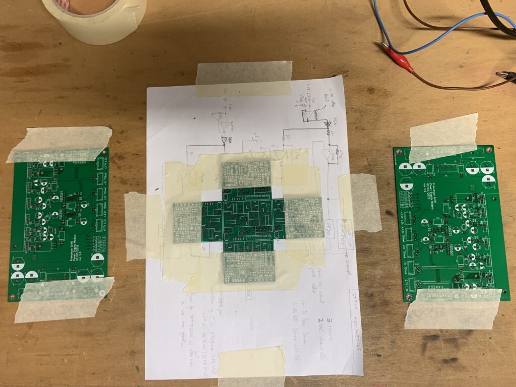
The PCB was reflowed using an hot-air gun
Testing and Results
And now to the most interesting parts: let’s see the filter in action!
I have tested it with different input signals at different frequenies, the following are some of the results
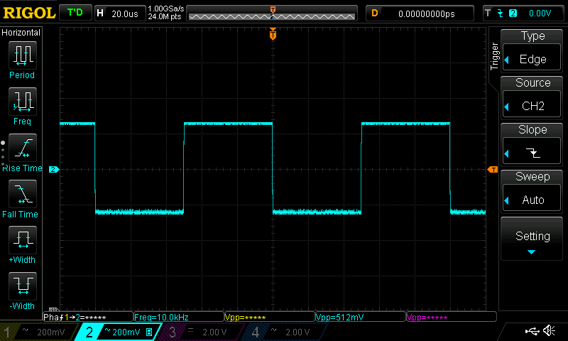
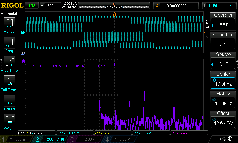
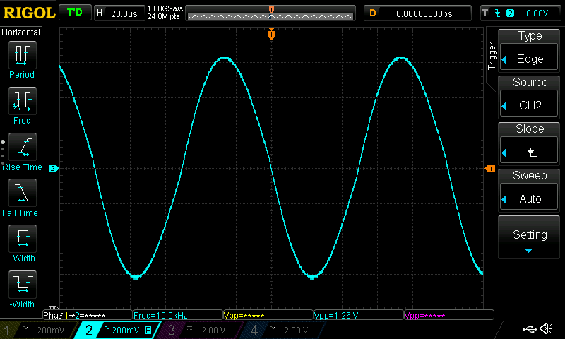
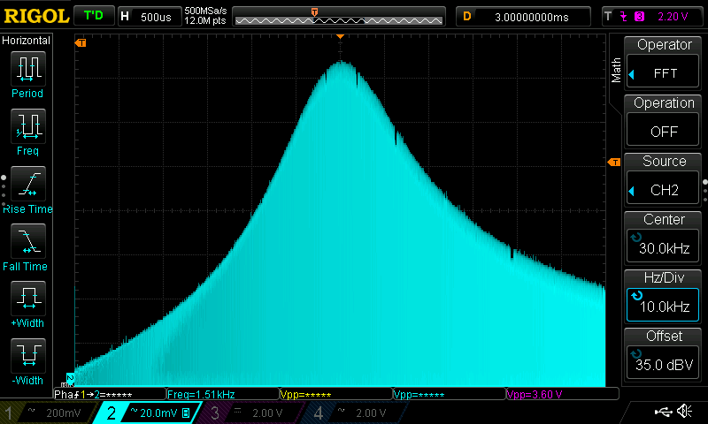
10kHz Square Wave
Here the filter frequency is set at 10kHz to extract the fundamental (sinusoid) component of the square wave
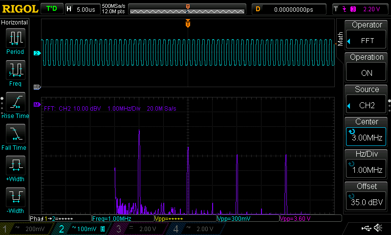
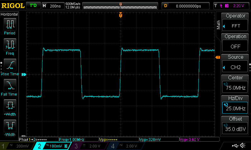
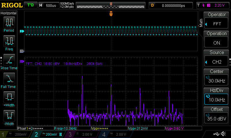
1MHz Square Qave
As previously the cutoff frequency is set at the same frequency of the fundamental harmonics of the input signal
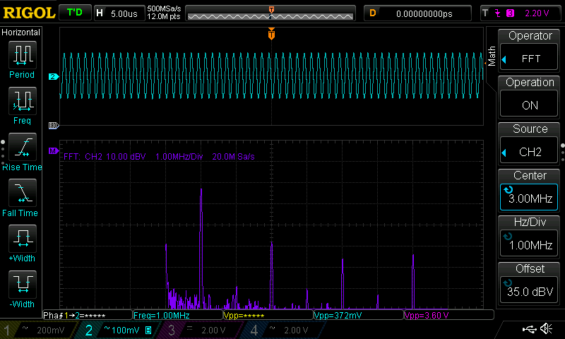
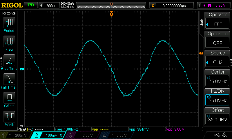
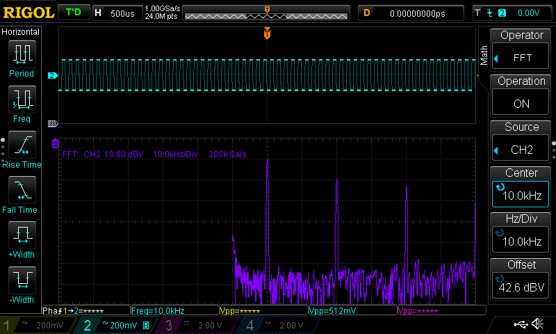
30kHz Square Wave
In this test the filter’s cutoff frequency wa set at the third harmonics of the input signal
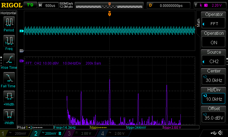
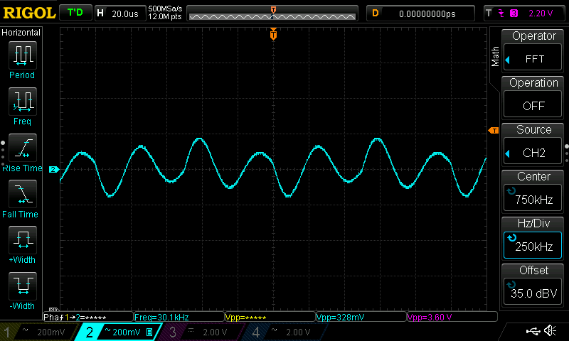
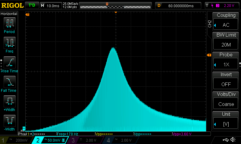
As the images show the outpt signal’s strongest component is now the one at 90kHz (which is the 3rd harmonics of the input signal). With a bit more filtering it would be possible to extract it very cleanly


